2015: Design Essentials
ESD Design Essentials
Date: January 8-9, 2015
Venue: The Oberoi, 39, Mahatma Gandhi Road, Bangalore, Karnataka - 56000, INDIA
Instructors: Harald Gossner, Intel; Prof. Mayank Shrivastava, Indian Institute of Science
This two-day workshop consists of concentrated versions of twelve ESD tutorials which comprise the following topics:
- ESD On-Chip Protection in Advanced Technologies
- SPICE-Based ESD Protection Design Utilizing Diodes and Active MOSFET Rail Clamp Circuits
- EOS/ESD Failure Models and Mechanisms
- On-Chip ESD Protection in RF Technologies
- Charged Device Model Phenomena and Design
- Latch-up Physics and Design
- Circuit Modeling and Simulation for On-Chip Protection
- Troubleshooting On-Chip ESD Failures
- Device Testing–IC Component Level: HBM, CDM, MM, and TLP
- Impact of Technology Scaling on ESD High Current Phenomena and Implications for Robust ESD Design
- Transmission Line Pulse
- Measurements: Parametric Analyzer for ESD On-Chip Protection
- System Level ESD/EMI: Testing to IEC and other Standards
Why to learn ESD Device and Circuit Design?
Predominant failure mechanism: It is estimated that above ~25% of component failures are due to Electrical Overstress (EOS) and Electrostatic Discharge (ESD).
Changing Technologies: Constantly changing technologies make the ESD protection design challenging. Learning from past Si technologies is no more sufficient.
Reliable Chips: For reliable operation of Integrated circuits ESD continues to be a major concern.

Programe details:
Day 1 (JAN. 8)
PART I (9:00 AM-1:00 PM) This part reviews the fundamentals of ESD testing, high-current physics, and ESD modeling. The focus is on device-level (HBM, CDM, MM, TLP) and system level testing, impact of technology scaling on ESD high current phenomena, as well as circuit modeling and simulation for on-chip protection.
PART II (2:00 PM-6:00 PM) The principles from part I are then applied to ESD Protection Design. This part describes ESD on-chip protection in advanced technologies, SPICE-based ESD protection design utilizing diodes, and active MOSFET rail clamp circuits.
Day 2 (JAN. 9)
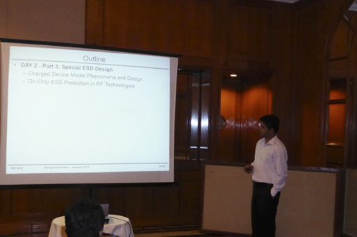
PART III (9:00 AM-1:00 PM) This part describes special ESD design cases, including Charged Device Model (CDM) phenomena and design, on-chip ESD protection in RF Technologies, and latch-up physics and design.
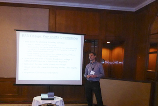
PART IV (2:00 PM-6:00 PM) The final section discusses EOS/ESD failure models and mechanisms. The seminar concludes with practical examples for troubleshooting of on-chip ESD failures.
This event is Co-Sponsored by the IEEE Local Chapter of Bangalore.